


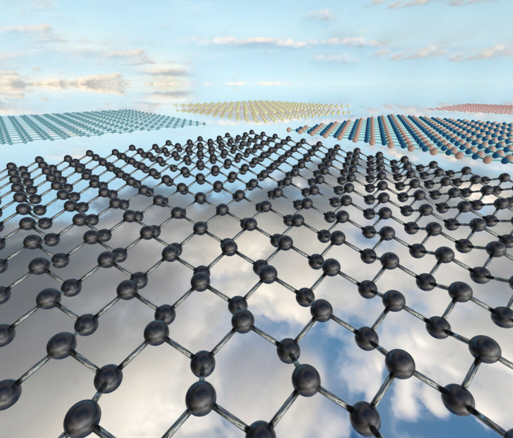
Dr Eng. Jakub Sitek, from the Faculty of Physics at the Warsaw University of Technology, together with an international group of researchers, has developed a new method that opens the door to mass production of devices based on 2D materials. The results of the team’s work have been published in ‘ACS Applied Materials & Interfaces’.
‘Our team has developed a method for the selective production of van der Waals heterostructures by chemical vapour deposition using electron beam irradiation’, says Dr Eng. Jakub Sitek and explains that the process involves exposing a substrate, such as graphene, to a very strong electron beam.
‘The electrons modify the substrate and at the same time saturate it with an electrical charge. We then grow another layer of 2D materials, e.g. semiconductors such as tungsten sulphide WS2, on this exposed substrate’, he adds.
Read more: